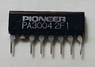

Chip pin specs are as follows:
Pin 1: Takes +12 to +14Vdc input. Chip should cease to function and Pin 3 should not go high if this voltage is not present. If voltage is below ~9.5V, the relay pin will fault.
Pin 3: Connects directly to the base of the relay that activates the protection relay. Voltage should go high (11.35V unloaded when Pin 1=12V) when no faiults are detected, but not until after the timing delay has elapsed. The base current sourced as to be sufficient to allow the relay to open! (at least 1mA base current)
Pin 4: Faults when detected DC offset is out of spec, causing the timing cap to discharge and Pin 3 to stay low. I measured the fault conditions to be V>0.28Vdc and V<-0.36Vdc. Current draw should be <100uA in both fault and non-fault conditions
Pin 5: connects to power supply board ground.
Pin 6: Faults when Vdc>-1.5V or open
Pin 7: Faults when VAC<1.5Vrms or open.
Pin 8: Connects to timing capacitor on the power supply board. Upon turn-on, voltage ramps up from 0V to ~8V. Once it gets to 8V, voltage clamps, and Pin 3 goes high, allowing the relay driver BJT to activate. Exact timing can be controlled by replacing the timing cap - a larger cap will increase the timing delay before the relay pulls in.